Bus and Memory Transfers
A digital system composed of many registers, and paths must be provided to transfer information from one register to another. The number of wires connecting all of the registers will be excessive if separate lines are used between each register and all other registers in the system.
A bus structure, on the other hand, is more efficient for transferring information between registers in a multi-register configuration system.
A bus consists of a set of common lines, one for each bit of register, through which binary information is transferred one at a time. Control signals determine which register is selected by the bus during a particular register transfer.
The following block diagram shows a Bus system for four registers. It is constructed with the help of four 4 * 1 Multiplexers each having four data inputs (0 through 3) and two selection inputs (S1 and S2).
We have used labels to make it more convenient for you to understand the input-output configuration of a Bus system for four registers. For instance, output 1 of register A is connected to input 0 of MUX1.
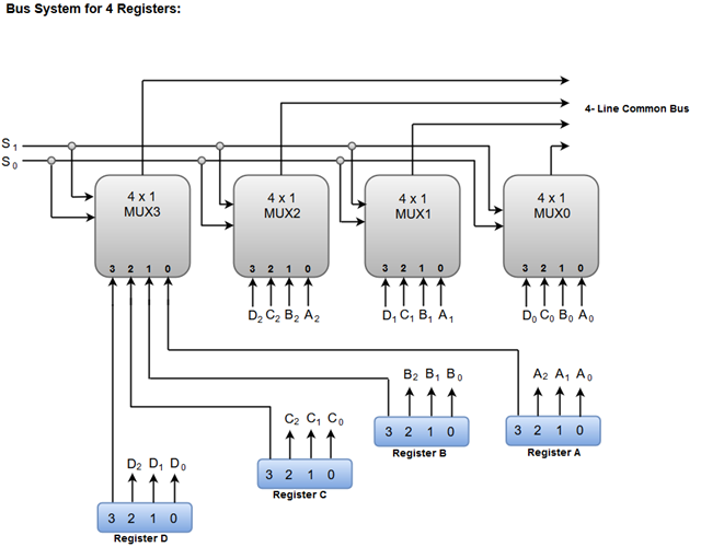
The two selection lines S1 and S2 are connected to the selection inputs of all four multiplexers. The selection lines choose the four bits of one register and transfer them into the four-line common bus.
When both of the select lines are at low logic, i.e. S1S0 = 00, the 0 data inputs of all four multiplexers are selected and applied to the outputs that forms the bus. This, in turn, causes the bus lines to receive the content of register A since the outputs of this register are connected to the 0 data inputs of the multiplexers.
Similarly, when S1S0 = 01, register B is selected, and the bus lines will receive the content provided by register B.
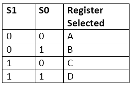
The following function table shows the register that is selected by the bus for each of the four possible binary values of the Selection lines.
Note: The number of multiplexers needed to construct the bus is equal to the number of bits in each register. The size of each multiplexer must be 'k * 1' since it multiplexes 'k' data lines. For instance, a common bus for eight registers of 16 bits each requires 16 multiplexers, one for each line in the bus. Each multiplexer must have eight data input lines and three selection lines to multiplex one significant bit in the eight registers.
A bus system can also be constructed using three-state gates instead of multiplexers.
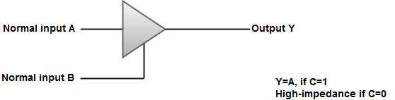
The three state gates can be considered as a digital circuit that has three gates, two of which are signals equivalent to logic 1 and 0 as in a conventional gate. However, the third gate exhibits a high-impedance state.
The most commonly used three state gates in case of the bus system is a buffer gate.
The graphical symbol of a three-state buffer gate can be represented as:
The following diagram demonstrates the construction of a bus system with three-state buffers.
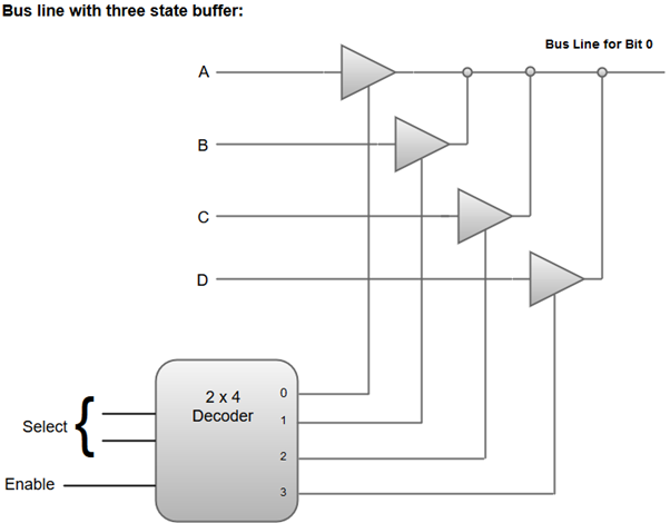
- The outputs generated by the four buffers are connected to form a single bus line.
- Only one buffer can be in active state at a given point of time.
- The control inputs to the buffers determine which of the four normal inputs will communicate with the bus line.
- A 2 * 4 decoder ensures that no more than one control input is active at any given point of time.
Memory Transfer
Most of the standard notations used for specifying operations on memory transfer are stated below.
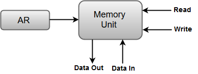
- The transfer of information from a memory unit to the user end is called a Read operation.
- The transfer of new information to be stored in the memory is called a Write operation.
- A memory word is designated by the letter M.
- We must specify the address of memory word while writing the memory transfer operations.
- The address register is designated by AR and the data register by DR.
- Thus, a read operation can be stated as:
- The Read statement causes a transfer of information into the data register (DR) from the memory word (M) selected by the address register (AR).
- And the corresponding write operation can be stated as:
- The Write statement causes a transfer of information from register R1 into the memory word (M) selected by address register (AR).
Ques. What is a memory transfer? What are different registers associated for memory transfer? Discuss.
Answer :
Memory Transfer:
The transfer of information from a memory word to the outside environment is called a read operation. The transfer of new information to be stored into the memory is called a write operation.
Different Registers Associated for Memory Transfer:
The address register (AR) is used to select a memory address, and the data register (DR) is used to send and receive data. Both these registers are connected to the internal bus.

DR← M[AR]:This is the read operation.
M[AR]<--R1:This is the write operation.
Ques. Explain the operation of three state bus buffers and show its use in design of common bus.
AKTU 2016-17, Marks 15
Answer :
Tri-State Buffers:
A tri-state buffer is a device that allows you to control when an output signal makes it to the bus. When the tri-state buffer's control bit is active, the input of the device makes it to the output. This is when the "valve" is open.
A three-state gate is a digital circuit that exhibits three states. Two of the states are signals equivalent to logic 1 and 0 as in a conventional gate. The third state is a high-impedance state.The high-impedance state behaves like an open circuit, which means that the output is disconnected and does not have a logic significance.

Used in designing Common Bus:

To form a single bus line, all the outputs of the 4 buffers are connected together.The control input will now decide which of the 4 normal inputs will communicate with the bus line.The decoder is used to ensure that only one control input is active at a time.Only one buffer would be in active state at any given interval of time.A bus system can be constructed with three state gates instead of multiplexer.A three state gate is a digital circuit that exhibits 3 states,2 of the states are signals equivalent to logic 1 and logic 0,the third state is a high impedance state(behaves like an open circuit which means that the output is disconnected and does not have a logic significance).
Ques. Explain why the single shared bus is so widely used as an interconnection medium in both sequential and parallel computers. What are its main disadvantages?
Answer :
Single Shared Bus:

Single Bus Structure:All units are connected to a single bus system.
Sequential Computers:Machine instructions are processed in a sequential manner and computers adopting this model are popularly called sequential computers
Parallel Computers:Parallel Computer Architecture is the method of organizing all the resources to maximize the performance and the programmability within the limits given by technology and the cost at any instance of time.
Disadvantages:
It has limited speed because only two units can participate in a data transfer at any given interval of time.
Ques. What is the benefit of using multiple bus architecture compared to a single bus architecture?
Answer :
Benefits of using multiple Bus Architecture are:
1. Reduces propagation delay,because each bus can be shorter.
2. Multiple buses permit several devices to work simultaneously, reducing time spent waiting and improving the computer's speed.
3. Performance improvements are the main reason for having multiple buses in a computer design.


No comments:
Post a Comment